- 您现在的位置:买卖IC网 > Sheet目录528 > UPA2731UT1A-E1-AY (Renesas Electronics America)MOSFET P-CH 30V 8-HVSON
�� ��
��
��DATA� SHEET�
�MOS� FIELD� EFFECT� TRANSISTOR�
�μ� PA2731UT1A�
�SWITCHING�
�P-CHANNEL� POWER� MOSFET�
�DESCRIPTION�
�The� μ� PA2731UT1A� is� P-channel� MOS� Field� Effect� Transistor� designed�
�for� power� management� applications� of� notebook� computers� and� Li-ion�
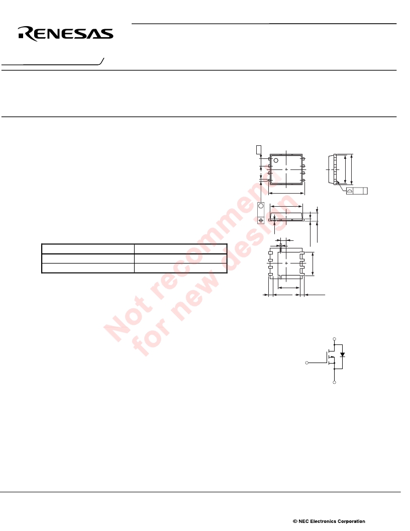
�PACKAGE� DRAWING� (Unit:� mm)�
�battery� protection� circuit.�
�1�
�2�
�8�
�7�
�FEATURES�
�?� Low� on-state� resistance�
�R� DS(on)1� =� 3.3� m� Ω� MAX.� (V� GS� =� ?� 10� V,� I� D� =� ?� 22� A)�
�R� DS(on)2� =� 6.4� m� Ω� MAX.� (V� GS� =� ?� 4.5� V,� I� D� =� ?� 22� A)�
�?� Low� C� iss� :� C� iss� =� 3620� pF� TYP.�
�?� Small� and� surface� mount� package� (8pin� HVSON)�
�3�
�4�
�6� ±� 0.2�
�5.4� ±� 0.2�
�6�
�5�
�0.10� S�
�ORDERING� INFORMATION�
�PART� NUMBER�
�PACKAGE�
�0.2�
�1�
�μ� PA2731UT1A-E1-AZ�
�μ� PA2731UT1A-E2-AZ�
�Note�
�Note�
�8pin� HVSON�
�8pin� HVSON�
�1,� 2,� 3� :� Source�
�4� :� Gate�
�5,� 6,� 7,� 8:� Drain�
�Note� Pb-free� (This� product� does� not� contain� Pb� in� external� electrode.)�
�3.65� ±� 0.2�
�ABSOLUTE� MAXIMUM� RATINGS� (T� A� =� 25� °� C,� All� terminals�
�are� connected.)�
�0.6� ±� 0.15�
�0.7� ±� 0.15�
�Drain� to� Source� Voltage� (V� GS� =� 0� V)� V� DSS�
�Gate� to� Source� Voltage� (V� DS� =� 0� V)� V� GSS�
�?� 30� V�
�m� 20� V�
�EQUIVALENT� CIRCUIT�
�Drain� Current� (pulse)�
�I� D(pulse)�
�Total� Power� Dissipation�
�P� T1�
�Total� Power� Dissipation� (PW� =� 10� sec)�
�P� T2�
�Single� Avalanche� Current�
�I� AS�
�Single� Avalanche� Energy�
�E� AS�
�Drain� Current� (DC)� I� D(DC)�
�Note1�
�Note2�
�Note2�
�Channel� Temperature� T� ch�
�Storage� Temperature� T� stg�
�Note3�
�Note3�
�m� 44� A�
�m� 180� A�
�1.5� W�
�4.6� W�
�°� C�
�150�
�?� 55� to� +150� °� C�
�?� 22� A�
�48� mJ�
�Gate�
�Drain�
�Source�
�Body�
�Diode�
�Notes� 1.� PW� ≤� 10� μ� s,� Duty� Cycle� ≤� 1%�
�2.� Mounted� on� a� glass� epoxy� board� (25.4� mm� x� 25.4� mm� x� 0.8� mm)�
�3.� Starting� T� ch� =� 25� °� C,� V� DD� =� ?� 15� V,� R� G� =� 25� Ω� ,� L� =� 100� μ� H,� V� GS� =� ?� 20� →� 0� V�
�Remark� Strong� electric� field,� when� exposed� to� this� device,� can� cause� destruction� of� the� gate� oxide� and� ultimately� degrade�
�the� device� operation.� Steps� must� be� taken� to� stop� generation� of� static� electricity� as� much� as� possible,� and�
�quickly� dissipate� it� once,� when� it� has� occurred.�
�The� information� in� this� document� is� subject� to� change� without� notice.� Before� using� this� document,� please�
�confirm� that� this� is� the� latest� version.�
�Not� all� products� and/or� types� are� available� in� every� country.� Please� check� with� an� NEC� Electronics�
�sales� representative� for� availability� and� additional� information.�
�Document� No.� G17640EJ1V0DS00� (1st� edition)�
�Date� Published� January� 2006� NS� CP(K)�
�Printed� in� Japan�
�2005�
�发布紧急采购,3分钟左右您将得到回复。
相关PDF资料
UPA2732UT1A-E1-AY
MOSFET LV 8HVSON
UPA2755AGR-E2-AT
MOSFET N-CH DUAL 30V 8-SOIC
UPA2756GR-E2-AT
MOSFET N-CH DUAL 60V 8-SOIC
UPA2757GR-E2-AT
MOSFET N-CH DUAL 30V 8-SOIC
UPA2790GR-E2-AT
MOSFET N/P-CH 30V 8-SOIC
UPA2791GR-E2-AT
MOSFET N/P-CH 30V 8-SOIC
UPA602T-T1-A
MOSFET N-CH DUAL 50V SC-59
UPA603T-T2-A
MOSFET P-CH DUAL 50V SC-59
相关代理商/技术参数
UPA2732UT1A-E1-AY
功能描述:MOSFET LV 8HVSON RoHS:是 类别:分离式半导体产品 >> FET - 单 系列:- 标准包装:1,000 系列:MESH OVERLAY™ FET 型:MOSFET N 通道,金属氧化物 FET 特点:逻辑电平门 漏极至源极电压(Vdss):200V 电流 - 连续漏极(Id) @ 25° C:18A 开态Rds(最大)@ Id, Vgs @ 25° C:180 毫欧 @ 9A,10V Id 时的 Vgs(th)(最大):4V @ 250µA 闸电荷(Qg) @ Vgs:72nC @ 10V 输入电容 (Ciss) @ Vds:1560pF @ 25V 功率 - 最大:40W 安装类型:通孔 封装/外壳:TO-220-3 整包 供应商设备封装:TO-220FP 包装:管件
UPA2735GR
制造商:RENESAS 制造商全称:Renesas Technology Corp 功能描述:P-channel MOSFET -30 V, -16 A, 5.0 m
UPA2735GR-E1-AT
制造商:RENESAS 制造商全称:Renesas Technology Corp 功能描述:P-channel MOSFET -30 V, -16 A, 5.0 m
UPA2735GR-E2-AT
制造商:RENESAS 制造商全称:Renesas Technology Corp 功能描述:P-channel MOSFET -30 V, -16 A, 5.0 m
UPA2736GR
制造商:RENESAS 制造商全称:Renesas Technology Corp 功能描述:P-channel MOSFET -30 V, -14 A, 7.0 m
UPA2736GR-E1-AT
制造商:RENESAS 制造商全称:Renesas Technology Corp 功能描述:P-channel MOSFET -30 V, -14 A, 7.0 m
UPA2736GR-E2-AT
制造商:RENESAS 制造商全称:Renesas Technology Corp 功能描述:P-channel MOSFET -30 V, -14 A, 7.0 m
UPA2737GR
制造商:RENESAS 制造商全称:Renesas Technology Corp 功能描述:P-channel MOSFET -30 V, -11 A, 13 m